In this study we prepared thin-film samples of the Fe2VAl-based Heusler phase by means of radio-frequency magnetron sputtering. The Fe2VAl-based Heusler phase was grown epitaxially, keeping the root-mean-square surface roughness smoother than 20 nm, even when the thickness of the samples exceeded 1000 nm. The composition of the samples was controlled via both target composition and the area of a small vanadium chip placed on the target. We succeeded in obtaining samples that were free from precipitation of a secondary phase. It was confirmed that the lattice thermal conductivity of the film samples can be reduced, irrespective of film thickness, and that the Seebeck coefficient was essentially the same as that of the bulk samples. These experimental results indicate that thin-film Fe2VAl-based Heusler alloys have potential as practical thermoelectric materials.
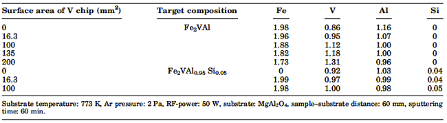
Figure 1 shows the temperature dependence of XRD patterns of films deposited on the MgAl2O4 substrate using the ternary Fe2VAl target. Samples deposited at room temperature give no peaks other than those of the substrate, so the deposited elements are assumed to form anamorphous phase. When the substrate temperature was increased to temperatures above 373 K the (2n 0 0) peaks of the Heusler phase appeared together with tiny peaks from an unknown secondary phase(s). The peak intensity from the Heusler phase increased with increasing substrate temperature. This unambiguously indicates that the quality of the structure of the Heusler phase was significantly improved by use of higher substrate temperature.
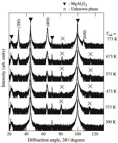
The root-mean-square (RMS) roughness of the deposited films shown in Fig. 2 indicates that a flat surface is obtainable by use of high-temperature substrates. We therefore selected 773 K, the highest stable substrate temperature of our system, for sample preparation. We also examined the substrate dependence and RF power-dependence of sample growth.
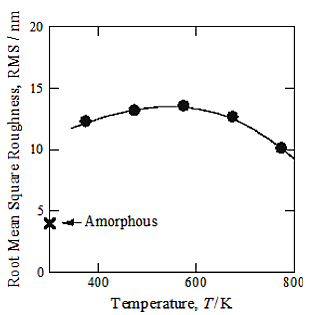
Figures 3a and b show XRD patterns obtained from samples deposited under different conditions. Obviously, even though the substrate and RF power were changed, the Fe2VAl- based Heusler phase grew as the dominant phase. It is also very important to note that the all the peaks from the Heusler phase were indexed as (2n 0 0). This indicates that the samples were deposited maintaining, at least, the single-axis orientation of the Heusler phase. To further investigate the structure of the film samples, we used XRD ![]() -scan measurements. The
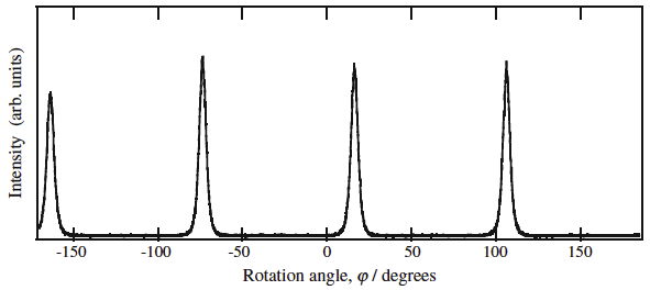
-scan measurements. The ![]() -scan pattern of the (2 2 0) peaks in Fig. 4 clearly shows four-fold-symmetry. This is definitely indicative of epitaxial growth of the Fe2VAl-based Heusler phase.
-scan pattern of the (2 2 0) peaks in Fig. 4 clearly shows four-fold-symmetry. This is definitely indicative of epitaxial growth of the Fe2VAl-based Heusler phase.
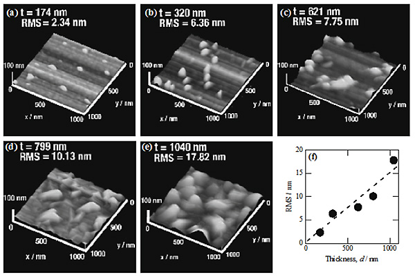
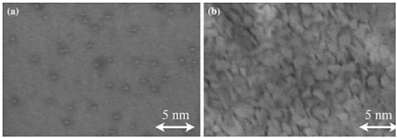
Figures 5a![]() e show AFM images of the film samples. The RMS roughness is plotted in Fig. 5f as a function of sample thickness. Corresponding SEM images are shown in Figs. 6a and b. The AFM images, the RMS roughness, and the SEM images clearly prove that the surface of the deposited sample was slightly roughened with increasing thickness. The SEM and AFM images showed island growth of the single crystalline Heusler phase. Nucleation of the single crystalline islands occurred on the very flat sample surface when the thickness of the samples was less than 200 nm. The size of the islands became larger with increasing thickness of the film, and the surface became rougher with growth of the islands.
e show AFM images of the film samples. The RMS roughness is plotted in Fig. 5f as a function of sample thickness. Corresponding SEM images are shown in Figs. 6a and b. The AFM images, the RMS roughness, and the SEM images clearly prove that the surface of the deposited sample was slightly roughened with increasing thickness. The SEM and AFM images showed island growth of the single crystalline Heusler phase. Nucleation of the single crystalline islands occurred on the very flat sample surface when the thickness of the samples was less than 200 nm. The size of the islands became larger with increasing thickness of the film, and the surface became rougher with growth of the islands.
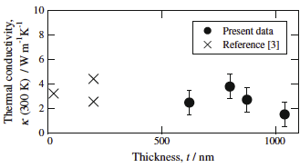
The thickness dependence of the thermal conductivity by using the epitaxial film composed solely of the Heusler phase are shown in Fig. 7. Obviously, the magnitude of the thermal conductivity was limited to a small value ![]() 4 Wm-1K-1, and the thermal conductivity was almost constant over the wide thickness range within measurement error. The average thermal conductivity was 3.0 ± 1.0 Wm-1K-1; this value can be compared with previously reported values of 2.57
4 Wm-1K-1, and the thermal conductivity was almost constant over the wide thickness range within measurement error. The average thermal conductivity was 3.0 ± 1.0 Wm-1K-1; this value can be compared with previously reported values of 2.57 ![]() 4.4 Wm-1K-1 for Fe2VAl-based Heusler alloy films 25
4.4 Wm-1K-1 for Fe2VAl-based Heusler alloy films 25 ![]() 200 nm thick.
200 nm thick.
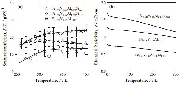
Figure 8a shows the temperature dependence of the Seebeck coefficient observed for films of Fe1.98V0.95Al1.07, Fe1.99V0.97Al0.99Si0.05, and Fe1.98V1.00Al0.98Si0.04, all with a thickness, t, ![]() 1000 nm. The observed Seebeck coefficient was positive in sign over the whole temperature range of measurement. The maximum magnitude of the Seebeck coefficient was less than 30
1000 nm. The observed Seebeck coefficient was positive in sign over the whole temperature range of measurement. The maximum magnitude of the Seebeck coefficient was less than 30 ![]() V/K, which is, unfortunately, much smaller than that observed for bulk samples. We considered this small magnitude was mainly because the sample compositions were different from those of the bulk samples with the largest Seebeck coefficient. The electrical resistivity of the samples shown in Fig. 8b decreased moderately with increasing temperature over the whole temperature range of measurement. The bulk samples behave similarly when the density of states at the Fermi level (
V/K, which is, unfortunately, much smaller than that observed for bulk samples. We considered this small magnitude was mainly because the sample compositions were different from those of the bulk samples with the largest Seebeck coefficient. The electrical resistivity of the samples shown in Fig. 8b decreased moderately with increasing temperature over the whole temperature range of measurement. The bulk samples behave similarly when the density of states at the Fermi level (![]() F) is very small in the presence of a pseudogap. The rather obvious increase in electrical resistivity with decreasing temperature observed at low temperatures, below 10 K, could be caused by the well-known Kondo effect in association with dilute magnetic impurities, although detailed analysis was not performed. The moderately decreasing electrical resistivity with increasing temperature could be caused by weak localization, which becomes significant for samples with both a small density of states at
F) is very small in the presence of a pseudogap. The rather obvious increase in electrical resistivity with decreasing temperature observed at low temperatures, below 10 K, could be caused by the well-known Kondo effect in association with dilute magnetic impurities, although detailed analysis was not performed. The moderately decreasing electrical resistivity with increasing temperature could be caused by weak localization, which becomes significant for samples with both a small density of states at ![]() F and a disordered atomic arrangement. We believe that the development of a weak localization effect at low temperature indicates the presence of disordering.
F and a disordered atomic arrangement. We believe that the development of a weak localization effect at low temperature indicates the presence of disordering.
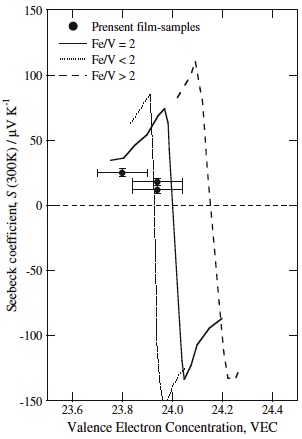
In Fig. 9 we have plotted the magnitude of the Seebeck coefficients for three samples, Fe1.98V0.95Al1.07, Fe1.99V0.97Al0.99Si0.05, and Fe1.98V1.00Al0.98Si0.04 as a function of VEC, together with previously reported universal lines for bulk samples. The data for the films were near the universal line for the bulk. This would indicate that the sputtering process does not seriously affect the Seebeck coefficient of the Fe2VAl- based Heusler alloys, and thick films of these alloys could be regarded as bulk materials, despite the fact that a very large Seebeck coefficient was not observed for these samples.